 Prakhar Gautam
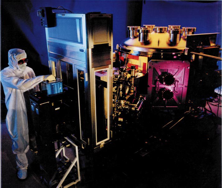
An ASML TWINSCAN EXE:5000 High-NA EUV scanner runs somewhere north of $380 million, and press coverage rounds that up to "$400 million" often enough that the number has basically stuck. It is an absurd machine: a plasma of molten tin droplets hit twice by a laser to make EUV light, a set of mirrors polished to sub-atomic smoothness because refractive lenses don't transmit 13.5nm light at all, and a wafer stage that positions to a fraction of a nanometer while moving. None of that engineering determines whether a given pattern actually resolves on the wafer. That's decided by a completely different discipline, running in a film maybe 20 nanometers thick: organometallic chemistry.
The industry's incumbent resist chemistry, chemically amplified resist (CAR), is running out of room at these dimensions. The replacement getting the most attention is a metal-oxide resist built around tin-oxo cage clusters — dodecameric organotin cages, roughly a nanometer across, that behave less like a polymer and more like a piece of inorganic coordination chemistry that happens to also be light-sensitive.
Why EUV can't just use a better CAR
Chemically amplified resist works by catalysis. A photon (or at longer wavelengths, a photon-driven exciton) triggers a photoacid generator, which releases a proton. That proton then diffuses through the resist film and catalytically deprotects the polymer backbone, changing its solubility — and because it's catalytic, one photon-triggered acid molecule can drive many deprotection events, which is where the "amplified" in the name comes from. That amplification is what made CAR sensitive enough to be practical at 193nm for two decades.
At EUV wavelengths the same trick becomes a liability. The acid has to diffuse to do its job, and diffusion doesn't know where the intended feature edge is supposed to be — it just blurs outward isotropically from wherever the acid was generated. At 193nm, with features tens of nanometers across, that blur was tolerable. At high-NA EUV pitches under 20nm, an acid diffusion length of even a few nanometers is a meaningful fraction of the entire feature, and it shows up directly as line-edge roughness. Worse, plain organic material — carbon, hydrogen, oxygen — is a weak EUV absorber to begin with, so CAR films need either more thickness or more incident dose to absorb enough photons in the first place, which drives cost and throughput in the wrong direction at exactly the moment the industry needs both to improve.
The photon isn't what does the chemistry
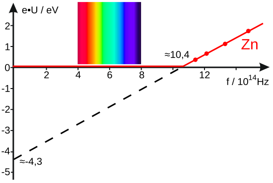
Here's the part that doesn't show up in most lithography explainers: an EUV photon at 13.5nm carries about 92 electron-volts, which is far more energy than any single chemical bond. That photon doesn't gently excite a molecule the way a visible or UV photon would. It ionizes an atom outright, ejecting a photoelectron with most of that 92 eV as kinetic energy. That primary photoelectron then scatters through the surrounding material, losing energy in a cascade of inelastic collisions and kicking out a shower of secondary electrons along the way — each one starting with only a few electron-volts, which happens to be right in the range that can break weak chemical bonds on contact. Recent work on tin-based resists puts the yield at somewhere between five and nine of these secondary electrons generated per absorbed EUV photon.
This means the actual bond-breaking chemistry in an EUV resist is done almost entirely by low-energy secondary electrons, not by the photon that started the cascade. It's the same physical regime electron-beam lithography operates in, which is part of why metal-oxide resists — originally developed for e-beam and helium-ion beam patterning — turned out to transfer so directly to EUV. The photon's only real job is picking the spot; the electrons do the work.
Why tin, specifically
Tin isn't an arbitrary choice of metal. At 92 eV, tin's photoabsorption is dominated by ionization of its 4d electrons, a resonance that happens to peak almost exactly at 13.5nm — measured photoionization cross sections put it around 11 megabarns per atom at that wavelength, and tin-oxo resist films have been measured absorbing up to three times more EUV light than equivalent organic CAR films. More tin in the beam path means more photons absorbed per nanometer of film, which means a thinner resist can still capture enough dose — directly easing the collapse and adhesion problems that plague ultra-thin organic films.
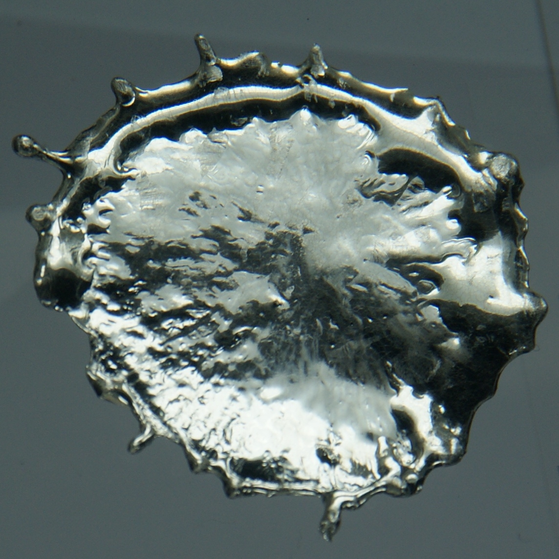
There's a nice bit of symmetry here that doesn't get mentioned often: this is the exact same 4d resonance that makes tin the EUV light source in the first place. Inside the scanner, a laser hits a droplet of liquid tin twice, first to shape it into a disk and then to blast it into a plasma of highly charged tin ions. Those ions have electron configurations that emit strongly clustered around 13.5nm as they relax — an unresolved transition array from 4p–4d and 4d–4f transitions. The element generating the light and the element absorbing it downstream in the resist are doing essentially the same 4d-electron physics, just running in opposite directions.
Development is a ligand-exchange reaction
The resist itself is typically a dodecameric tin-oxo cage, formulated roughly as [(RSn)12O14(OH)6]X2 — twelve tin centers bridged by oxo and hydroxo groups into a compact cage, each tin also carrying an organic ligand (R) and a counter-anion (X) that keep the whole cluster soluble in an organic casting solvent. Spin-coat it onto the wafer as a thin, dense film and it sits there, fully soluble, until it gets hit.
Where a secondary electron lands, it homolyzes a weak Sn–ligand bond — the sensitivity of a given cluster correlates directly with how weak that Sn–C bond is — kicking off a reactive, Lewis-acidic tin center with the ligand gone. That exposed tin site doesn't sit still. It condenses with a neighboring cluster's oxo or hydroxo group, forming a new Sn–O–Sn bridge, promoted along by ambient moisture. Do that across enough clusters in the exposed region and you've converted a shell of individually soluble organotin cages into one continuous, cross-linked, inorganic tin-oxide network. That network doesn't dissolve in the same organic solvent the unexposed cage material does.
"Development," in other words, isn't dissolving away material that reacted — it's rinsing away material that didn't. The exposed regions survive because ligand exchange and condensation converted them into an inorganic network; the unexposed regions wash off because they're still just soluble organotin cage clusters. It's a negative-tone process, and the chemistry doing the pattern-defining work is a ligand-substitution and condensation reaction straight out of inorganic coordination chemistry, not a solubility switch in a polymer backbone.
This is also the real chemical difference between CAR and metal-oxide resist, and it's not really about the metal at all — it's about amplification. CAR is catalytic: one acid-generating event drives many deprotection events, which is a gain in sensitivity and a source of blur, because the catalyst diffuses before it's done reacting. A tin-oxo cage is closer to stoichiometric: each secondary electron does roughly one ligand-loss event, right where it landed, with no diffusing catalyst to blur the edge. You trade some raw sensitivity for spatial precision, which is exactly the trade High-NA needs made.
The stochastic problem doesn't go away — it moves
Higher absorption cross section means fewer incident photons are needed to deposit a given dose, which directly helps the most basic stochastic problem in EUV: shot noise. Dose is ultimately a photon count, and photon arrival is a Poisson process — at the pitches High-NA is targeting, a given feature's edge is defined by a genuinely small number of absorption events, small enough that the statistical variance in that count is no longer negligible. Some pixels, purely by chance, don't accumulate enough exposure. That shows up as missing contacts, bridged lines, and edge roughness that no amount of overlay or focus correction can fix, because the problem isn't systematic error — it's randomness baked into how few particles are actually doing the counting.
Metal-oxide resist's high absorption cross section directly improves this by requiring a lower dose for equivalent signal — published figures put tin-oxo resists at roughly 4x better photon efficiency than conventional CAR for equivalent shot noise. But the secondary-electron cascade that makes the chemistry work is itself a second, independent source of randomness, and it doesn't shrink the same way. Each absorbed photon kicks out a variable number of secondary electrons — that five-to-nine range isn't a fixed number, it's a distribution — and industry analysis of that variability has found it converges toward roughly a 61% coefficient of variation as dose increases, meaning past a certain point, more dose stops meaningfully reducing edge placement error. At a 20nm half-pitch, electron-count fluctuation alone has been estimated at close to 50% variation. Fixing the photon-shot-noise problem, in other words, doesn't fix the actual noise floor — it just reveals the next one sitting underneath it.
What I'd watch
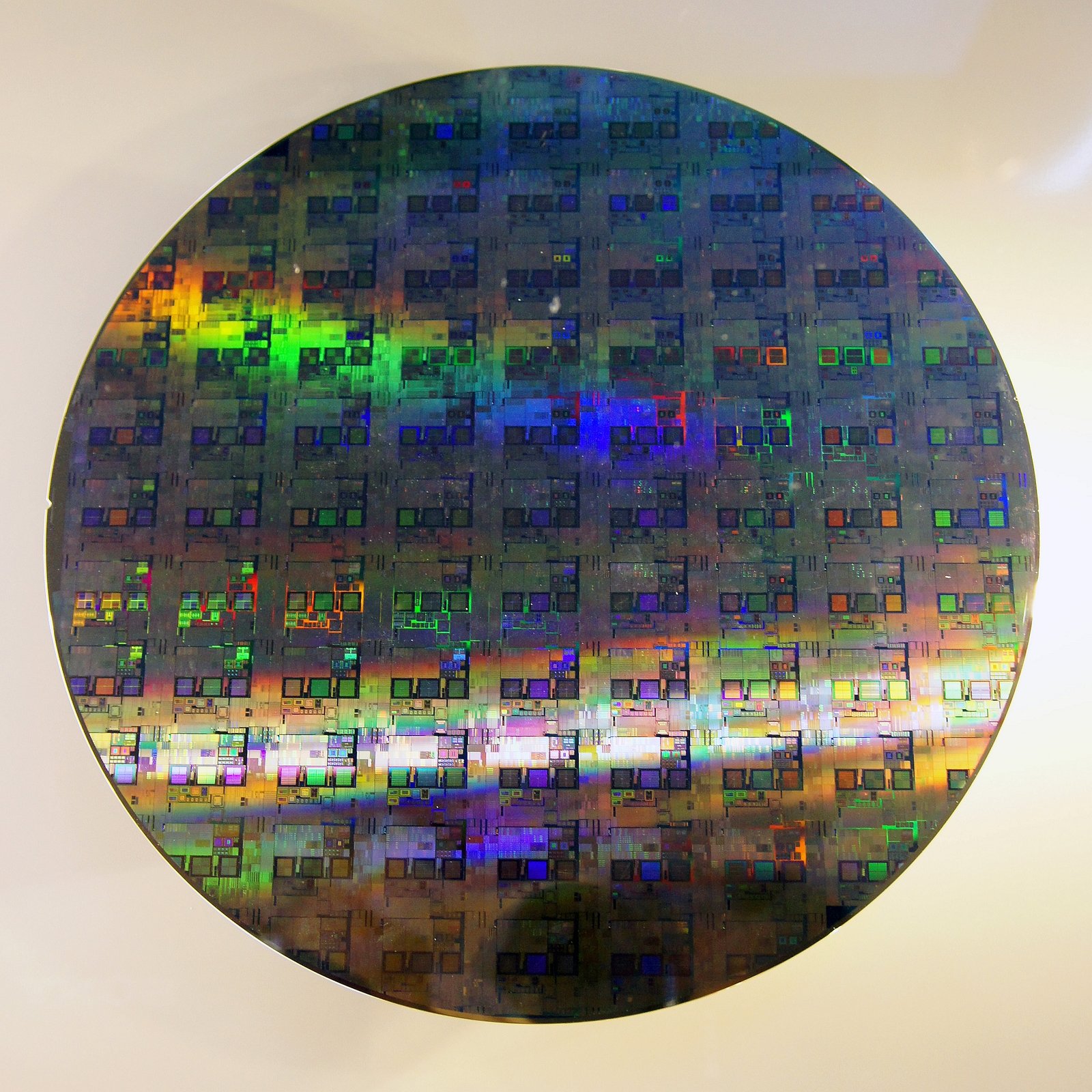
Whether the secondary-electron noise floor turns out to be a hard physical limit or just the next problem chemists find a way to design around — cluster geometry, ligand choice, and counter-ion selection all shift the electron yield and cross-linking efficiency, so there's real room to tune the chemistry rather than just the dose. Whether metal-oxide resist actually displaces CAR in production at scale or stays a High-NA specialty material, given how much qualification and defect-inspection infrastructure the industry has built around decades of chemically amplified chemistry. And, honestly, whether more people clock that the thing standing between a $400 million machine and a working chip is a rinse step built on ligand exchange — an organotin cage molecule quietly doing the same kind of chemistry you'd find in a coordination chemistry course, at the most expensive manufacturing step humans currently run.
The scanner gets the headlines. The chemistry decides whether the pattern actually shows up.
Further reading
- Cardineau, B., Del Re, R., Marnell, M., Al-Mashat, H., Vockenhuber, M., Ekinci, Y., Sarma, C., Freedman, D.A., & Brainard, R.L. "Photolithographic properties of tin-oxo clusters using extreme ultraviolet light (13.5 nm)." Microelectronic Engineering, 127, 44–50 (2014). DOI: 10.1016/j.mee.2014.04.024
- Fallica, R., Haitjema, J., Wu, L., Castellanos Ortega, S., Brouwer, A.M., & Ekinci, Y. "Absorption coefficient of metal-containing photoresists in the extreme ultraviolet." Journal of Micro/Nanolithography, MEMS, and MOEMS, 17(2), 023505 (2018). DOI: 10.1117/1.JMM.17.2.023505
- Bespalov, I., Zhang, Y., Haitjema, J., Tromp, R.M., van der Molen, S.J., Brouwer, A.M., Jobst, J., & Castellanos, S. "Key Role of Very Low Energy Electrons in Tin-Based Molecular Resists for Extreme Ultraviolet Nanolithography." ACS Applied Materials & Interfaces, 12(8), 9881–9889 (2020). DOI: 10.1021/acsami.9b19004
- Versolato, O.O. "Physics of laser-driven tin plasma sources of EUV radiation for nanolithography." Plasma Sources Science and Technology, 28(8), 083001 (2019). DOI: 10.1088/1361-6595/ab3302
- Hasan, M.W., Deeb, L., Kumaniaev, S., Wei, C., & Wang, K. "Recent Advances in Metal-Oxide-Based Photoresists for EUV Lithography." Micromachines, 15(9), 1122 (2024). Open access. DOI: 10.3390/mi15091122
- Chen, F.T. "How Secondary Electrons Worsen EUV Stochastics." Exposing EUV (2025). frederickchen.substack.com
- Inpria Corporation. Metal oxide photoresist technology overview. inpria.com
- ASML. "TWINSCAN EXE:5000." Product documentation. asml.com
- "ASML's High-NA chipmaking tool will cost $380 million." Tom's Hardware. tomshardware.com
- "New Challenges Emerge With High-NA EUV." Semiconductor Engineering. semiengineering.com